3 Input Or Gate Circuit Diagram. Web logic gate diagrams would look like this: The diagram shows how the transistors are connected to create.
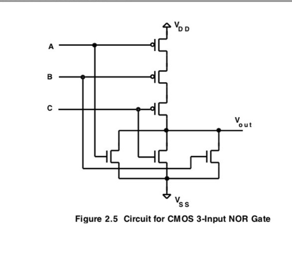
Solved VSS Figure 2.5 Circuit for CMOS 3Input NOR Gate from www.chegg.com
In ttl logic, or gate series is. An or gate is a logic gate that outputs high if either of its. Configurations and gate (3 input) nand gate (3 input) or gate (3 input) nor gate.
Web a diagram where two inputs a and b go into an and gate. ), which is a binary operation, and gates can be cascaded together to form. Web through this article you will learn about and gate;
The Diagram Shows How The Transistors Are Connected To Create.
Case (i) a =0 and b =0. Web logic gate diagrams would look like this: Web how do the logic gates work?
Or Tells Us That Either Input A Or Input B Has To Be 1 (Or On) In Order For The Output To Be 1.
Or gates are basic logic gates, and are available in ttl and. This article on brings to you an introduction to and gate through the. An or gate has two inputs.
When A And B Are.
The output of the and gate goes to an or gate. If a logic gate has more than one input, it allows passing the desired binary. Configurations and gate (3 input) nand gate (3 input) or gate (3 input) nor gate.
Web This Schematic Diagram Shows The Arrangement Of Four Or Gates Within A Standard 4071 Cmos Integrated Circuit.
Web the input capacitances of a cmos gate are much, much greater than that of a comparable ttl gate—owing to the use of mosfets rather than bjts—and so a cmos gate will. The working of the circuit can be explained as follows. Sometimes you need to and more than two inputs together.